
Microprocessor
Definition: A microprocessor is a central processing unit (CPU) on a single integrated circuit (IC) that performs the logic and arithmetic functions of a computer.
Key Features:
- CPU-Centric: Primarily focuses on computation and data processing.
- External Components: Requires external components such as memory (RAM, ROM), input/output ports, and peripherals to function.
- Versatility: Can be used in a variety of applications by connecting different peripheral devices and memory units.
- Complex Tasks: Suitable for complex and high-performance tasks like personal computing, data processing, and running operating systems.
- General Purpose: Typically used in devices requiring significant computational power and flexibility, such as desktops, laptops, and servers.
Examples: Intel Core i7, AMD Ryzen, ARM Cortex-A series.
Microcontroller
Definition: A microcontroller is a compact integrated circuit designed to govern a specific operation in an embedded system. It includes a CPU, memory, and input/output peripherals on a single chip.
Key Features:
- Integrated System: Combines CPU, RAM, ROM (or Flash), I/O ports, timers, and other peripherals on a single chip.
- Specialized Tasks: Designed for specific control-oriented tasks, often in embedded systems.
- Compact and Efficient: Optimized for controlling specific devices and performing dedicated functions with low power consumption.
- Ease of Use: Simplifies the design of control systems because of its integrated nature, reducing the need for additional external components.
- Cost-Effective: Typically less expensive than microprocessors due to integration and specific application design.
Examples: Atmel AVR, Microchip PIC, ARM Cortex-M series.
Comparison Between Microprocessor and Microcontroller
- Components:
- Microprocessor: Requires external components for memory (RAM, ROM), and I/O operations, resulting in a more complex and larger circuit board.
- Microcontroller: Integrates all necessary components (CPU, memory, I/O) on a single chip, simplifying the overall design and reducing space.
- Application Scope:
- Microprocessor: Used in high-end computing devices such as personal computers, workstations, and servers where extensive computational tasks and multi-tasking are required.
- Microcontroller: Used in embedded systems such as home appliances, automotive systems, medical devices, and industrial machinery, where specific, repetitive tasks are needed.
- Power Consumption:
- Microprocessor: Generally consumes more power due to higher computational capabilities and the need for multiple external components.
- Microcontroller: Designed for low power consumption, making it suitable for battery-operated devices and applications where energy efficiency is critical.
- Cost:
- Microprocessor: Higher cost due to the need for external components and the complexity of the applications it supports.
- Microcontroller: Lower cost because of integrated components and the focused nature of its applications.
- Performance:
- Microprocessor: Higher performance capabilities suitable for complex applications that require significant processing power.
- Microcontroller: Performance is optimized for specific control-oriented tasks rather than general-purpose computing.
Practical Examples:
- Microprocessor: Used in personal computers, gaming consoles, and servers where a wide range of applications and multitasking are required.
- Microcontroller: Used in microwave ovens, washing machines, remote controls, automotive engine control units (ECUs), and wearable devices where specific control tasks are performed efficiently.
8086 Microprocessor
8086 Microprocessor is an enhanced version of 8085 Microprocessor that was designed by Intel in 1976. It is a 16-bit Microprocessor having 20 address lines and 16 data lines that provides up to 1MB storage.
- The architecture of the 8086 microprocessor is based on a complex instruction set computer (CISC) architecture.
- The 8086 microprocessor has a 20-bit address bus, which can address up to 1 MB of memory, and a 16-bit data bus, which can transfer data between the microprocessor and memory or I/O devices.
Features of the 8086 Microprocessor
- 16-bit Processor: The 8086 is a 16-bit microprocessor, meaning it can process 16 bits of data at a time.
- Clock Speed: The 8086 operates at clock speeds ranging from 5 MHz to 10 MHz.
- Address Bus: It has a 20-bit address bus, allowing it to address 1 MB of memory directly (2^20 addresses).
- Data Bus: The data bus is 16 bits wide, enabling faster data transfer compared to 8-bit processors.
- Registers: The 8086 includes a set of 16-bit registers, including general-purpose registers, segment registers, a pointer register, and an index register.
- Instruction Set: The processor supports a rich instruction set, including arithmetic, logical, control, and string operations.
- Pipeline Architecture: It uses a simple instruction pipeline to overlap fetch and execute operations, enhancing performance.
- Interrupt System: The 8086 has an advanced interrupt system with both hardware and software interrupts.
- Segmentation: Memory is divided into segments, each up to 64 KB in size, allowing for more efficient memory management.
- Compatibility: It maintains backward compatibility with the 8080 and 8085 microprocessors.
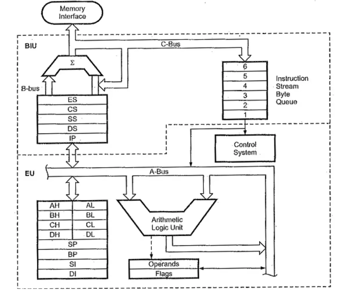
Architecture of the 8086 Microprocessor
The architecture of the 8086 can be divided into two main units:
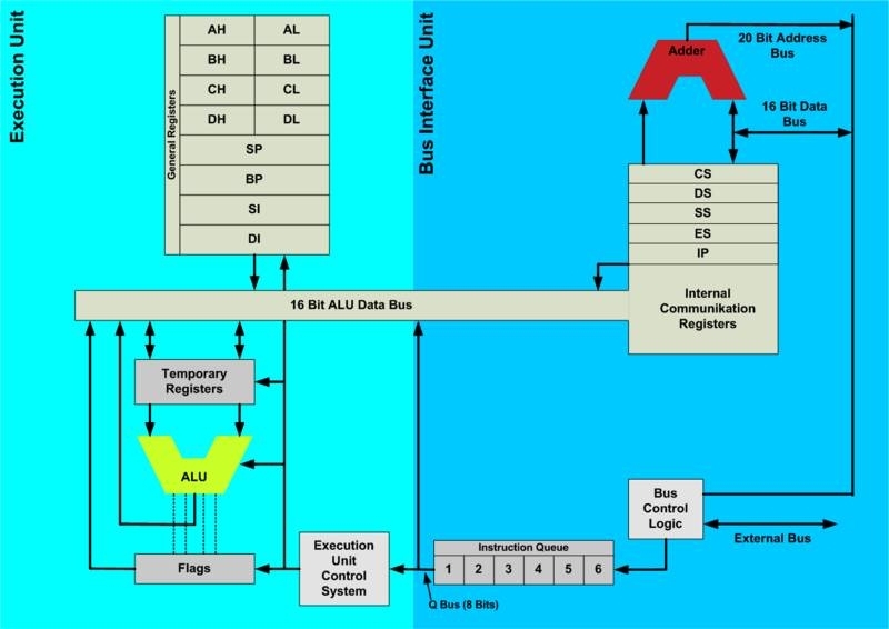
1 Execution Unit (EU):
It is responsible for decoding and executing instructions fetched from memory by the Bus Interface Unit (BIU). The EU handles arithmetic, logical, and control operations, utilizing various internal registers and the Arithmetic Logic Unit (ALU).
Execution unit gives instructions to BIU stating from where to fetch the data and then decode and execute those instructions. Its function is to control operations on data using the instruction decoder & ALU. EU has no direct connection with system buses as shown in the above figure, it performs operations over data through BIU.
The Execution Unit (EU) in the 8086 microprocessor is like the worker that does the actual tasks. Imagine it as the hands and brain of the microprocessor, taking care of instructions and calculations. Here’s a simple breakdown:
1. Telling BIU What to Do:
The EU is like the supervisor. It communicates with the Bus Interface Unit (BIU) to let it know where to fetch instructions or data from. It’s like giving directions to the person in charge of fetching information.
2. Understanding Instructions:
The EU is like a translator. It takes the instructions fetched from the memory by the BIU and figures out what actions to perform. It decodes the instructions, making them understandable. It’s similar to translating a set of instructions into tasks that can be done.
3. Performing Actions:
Inside the EU, there’s something called the Arithmetic Logic Unit (ALU). Think of the ALU as a small calculator. It performs actions like adding, subtracting, and making logical decisions based on the instructions decoded by the EU. It’s like the hands that carry out the tasks.
4. Flags and Decisions:
The EU uses the ALU to perform calculations, and based on the results, it sets or clears flags in the FLAG Register. These flags, like the Overflow Flag (OF) or Zero Flag (ZF), help the microprocessor make decisions about what to do next. It’s like the worker telling the supervisor if everything went well or if there’s a problem.
Components of the Execution Unit:
1 General Purpose Registers:
There are 8 general purpose registers, i.e., AH, AL, BH, BL, CH, CL, DH, and DL. These registers can be used individually to store 8-bit data and can be used in pairs to store 16 bit data. The valid register pairs are AH and AL, BH and BL, CH and CL, and DH and DL. It is referred to the AX, BX, CX, and DX respectively.
- AX (Accumulator Register): Primarily used for arithmetic, logic, and data transfer operations. It can be divided into two 8-bit registers: AL (lower 8 bits) and AH (upper 8 bits).
- BX (Base Register): Often used for indexed addressing and can be split into BL and BH.
- CX (Count Register): Used for loop and string operations, also split into CL and CH.
- DX (Data Register): Used in I/O operations and as a part of some arithmetic operations, split into DL and DH.
2 Flag Register:
It is a 16-bit register that behaves like a flip-flop, i.e. it changes its status according to the result stored in the accumulator. It has 9 flags and they are divided into 2 groups − Conditional Flags and Control Flags.
Conditional Flags: It represents the result of the last arithmetic or logical instruction executed. Following is the list of conditional flags −
- Carry flag − This flag indicates an overflow condition for arithmetic operations.
- Auxiliary flag − When an operation is performed at ALU, it results in a carry/barrow from lower nibble (i.e. D0 – D3) to upper nibble (i.e. D4 – D7), then this flag is set, i.e. carry given by D3 bit to D4 is AF flag. The processor uses this flag to perform binary to BCD conversion.
- Parity flag − This flag is used to indicate the parity of the result, i.e. when the lower order 8-bits of the result contains even number of 1’s, then the Parity Flag is set. For odd number of 1’s, the Parity Flag is reset.
- Zero flag − This flag is set to 1 when the result of arithmetic or logical operation is zero else it is set to 0.
- Sign flag − This flag holds the sign of the result, i.e. when the result of the operation is negative, then the sign flag is set to 1 else set to 0.
- Overflow flag − This flag represents the result when the system capacity is exceeded.
Control Flags: Control flags controls the operations of the execution unit. Following is the list of control flags −
- Trap flag − It is used for single step control and allows the user to execute one instruction at a time for debugging. If it is set, then the program can be run in a single step mode.
- Interrupt flag − It is an interrupt enable/disable flag, i.e. used to allow/prohibit the interruption of a program. It is set to 1 for interrupt enabled condition and set to 0 for interrupt disabled condition.
- Direction flag − It is used in string operation. As the name suggests when it is set then string bytes are accessed from the higher memory address to the lower memory address and vice-a-versa.
– Working of the Execution Unit:
- Fetching:
- Although primarily the BIU's responsibility, the EU coordinates with the BIU to fetch the next instruction from the instruction queue.
- The EU is like the supervisor. It communicates with the Bus Interface Unit (BIU) to let it know where to fetch instructions or data from. It’s like giving directions to the person in charge of fetching information.
- Decoding:
- The instruction decoder within the EU decodes the fetched instruction to understand what action needs to be taken.
- The EU is like a translator. It takes the instructions fetched from the memory by the BIU and figures out what actions to perform. It decodes the instructions, making them understandable. It’s similar to translating a set of instructions into tasks that can be done.
- Operand Fetching:
- If the instruction requires operands (data), the EU fetches these from registers or memory.
- Execution:
- The ALU performs the required operation (e.g., arithmetic, logic) on the operands.
- Inside the EU, there’s something called the Arithmetic Logic Unit (ALU). Think of the ALU as a small calculator. It performs actions like adding, subtracting, and making logical decisions based on the instructions decoded by the EU. It’s like the hands that carry out the tasks.
- Result Storage:
- The result of the operation is stored back in the appropriate register or memory location.
- Updating Flags:
- The status flags in the flag register are updated based on the result of the operation.
- The EU uses the ALU to perform calculations, and based on the results, it sets or clears flags in the FLAG Register. These flags, like the Overflow Flag (OF) or Zero Flag (ZF), help the microprocessor make decisions about what to do next. It’s like the worker telling the supervisor if everything went well or if there’s a problem.
2 Bus Interface Unit (BIU):
It handles all the interactions between the processor and external memory and I/O devices. The BIU works in conjunction with the Execution Unit (EU) to fetch, decode, and execute instructions efficiently.
BIU takes care of all data and addresses transfers on the buses for the EU like sending addresses, fetching instructions from the memory, reading data from the ports and the memory as well as writing data to the ports and the memory. EU has no direction connection with System Buses so this is possible with the BIU. EU and BIU are connected with the Internal Bus.
Functions of the Bus Interface Unit
- Instruction Fetching: The BIU is responsible for fetching instructions from memory. It pre-fetches instructions and stores them in a queue, allowing the EU to execute instructions concurrently, thereby improving processing efficiency.
- Memory Address Calculation: The BIU calculates physical addresses for memory operations using segment and offset values.
- Data Transfer: It manages the transfer of data between the processor and memory or I/O devices via the data bus.
- Bus Control: The BIU controls the use of the address and data buses, ensuring that the correct data is read from or written to the appropriate memory locations or I/O ports.
- Segment Management: It uses segment registers to handle memory segmentation, a technique that divides memory into manageable sections.
Components of the Bus Interface Unit:
1 Segment Registers:
BIU has 4 segment buses, i.e. CS, DS, SS& ES. It holds the addresses of instructions and data in memory, which are used by the processor to access memory locations. It also contains 1 pointer register IP, which holds the address of the next instruction to executed by the EU.
- CS − It stands for Code Segment. It is used for addressing a memory location in the code segment of the memory, where the executable program is stored.
- DS − It stands for Data Segment. It consists of data used by the program and is accessed in the data segment by an offset address or the content of other register that holds the offset address.
- SS − It stands for Stack Segment. It handles memory to store data and addresses during execution.
- ES − It stands for Extra Segment. ES is additional data segment, which is used by the string to hold the extra destination data.
2 Instruction Queue:
BIU contains the instruction queue. BIU gets up to 6 bytes of next instructions and stores them in the instruction queue. When EU executes instructions and is ready for its next instruction, then it simply reads the instruction from this instruction queue resulting in increased execution speed.
- Fetching the next instruction while the current instruction executes is called pipelining.
- This pipelining increases the overall efficiency of the microprocessor.
3 Bus Control Logic:
- Manages control signals for memory and I/O operations, ensuring that the correct operation (read or write) is performed at the right time.
4 Address and Data Buses:
- Address Bus: A 20-bit bus used to address memory locations, enabling the 8086 to access up to 1 MB of memory.
- Data Bus: A 16-bit bus used for data transfer between the processor, memory, and I/O devices.
Operations of the Bus Interface Unit
- Instruction Fetching and Queuing:
- The BIU fetches the next instruction from memory using the segment and offset addresses, storing it in the instruction queue. While the EU executes one instruction, the BIU can fetch the next instruction, enabling overlap and pipelining.
- Address Calculation:
- Physical addresses are calculated by combining a segment base address with an offset address. The formula used is:
Physical Address=(Segment Base×16)+Offset - For example, if the CS register contains 0x1234 and the IP register (instruction pointer) contains 0x5678, the physical address for the next instruction fetch would be:
(0x1234×16)+0x5678=0x12340+0x5678=0x179B8
- Physical addresses are calculated by combining a segment base address with an offset address. The formula used is:
- Data Transfer:
- For data read and write operations, the BIU uses the calculated physical addresses to access memory or I/O devices. The BIU ensures that data is correctly placed on or retrieved from the data bus.
- Bus Control:
- The BIU generates control signals such as Memory Read (MR), Memory Write (MW), I/O Read (IOR), and I/O Write (IOW) to coordinate data transfers.
- It ensures proper timing and sequence of operations to avoid conflicts on the address and data buses.
Interaction with Execution Unit
The BIU and EU work in parallel to maximize efficiency:
- Parallel Processing:
- While the EU executes the current instruction, the BIU fetches the next instruction and places it in the queue. This parallelism is facilitated by the instruction queue, allowing overlap of fetch and execute phases.
- Segmentation Handling:
- The BIU manages segmentation transparently to the EU, allowing the EU to focus on instruction execution without worrying about address calculations.

Leave a comment
Your email address will not be published. Required fields are marked *