
Architecture Overview
The basic components of a computer include a Central Processing Unit (CPU), Primary Storage or Random Access Memory (RAM), Secondary Storage, Input/Output devices (e.g., screen, keyboard, mouse), and an interconnection referred to as the Bus.
A very basic diagram of the computer architecture is as follows:
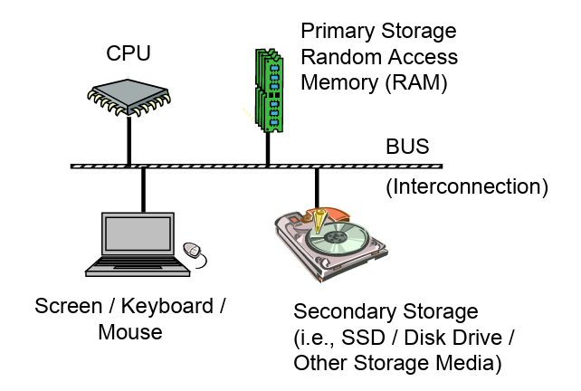
Computer Architecture

The architecture is typically referred to as the Von Neumon Architecture or the Princeton architecture, and was described in 1945 by the mathematician and physicist John von Neumann.
Programs and data are typically stored on secondary storage (e.g., disk drive or solid state drive). When a program is executed, it must be copied from secondary storage into the primary storage or main memory (RAM). The CPU executes the program from primary storage or RAM.
Primary storage or main memory is also referred to as volatile memory since when power is removed, the information is not retained and thus lost. Secondary storage is referred to as non-volatile memory since the information is retained when powered off.
For example, consider storing a term paper on secondary storage (i.e., disk). When the user starts to write or edit the term paper, it is copied from the secondary storage medium into primary storage (i.e., RAM or main memory). When done, the updated version is typically stored back to the secondary storage (i.e., disk). If you have ever lost power while editing a document (assuming no battery or uninterruptible power supply), losing the unsaved work will certainly clarify the difference between volatile and non-volatile memory.
Data Storage Sizes
The x86-64 architecture supports a specific set of data storage size elements, all based on powers of two. The supported storage sizes are as follows:
| Storage | Size (bits) | Size (bytes) |
| Byte | 8-bits | 1 byte |
| Word | 16-bits | 2 bytes |
| Double-word | 32-bits | 4 bytes |
| Quadword | 64-bits | 8 bytes |
| Double quadword | 128-bits | 16 bytes |
These storage sizes have a direct correlation to variable declarations in high-level languages (e.g., C, C++, Java, etc.).
Components of CPU Architecture
1 Control Unit (CU):
It fetches instructions from memory, decodes them, and then manages their execution by coordinating with the ALU, registers, and other components.
2 Arithmetic Logic Unit (ALU):
The arithmetic logic unit is the computational engine of the CPU. It performs arithmetic operations (such as addition, subtraction, multiplication, and division) as well as logical operations (such as AND, OR, and NOT) on data received from memory or registers.
3 Registers:
Registers are small, high-speed storage units located within the CPU. They serve as temporary storage locations for data and instructions during processing. Registers play a crucial role in speeding up computations by providing fast access to frequently used data and instructions. Common types of registers include the Program Counter (PC), Instruction Register (IR), and General-Purpose Registers (e.g., AX, BX, CX, DX in x86 architecture).
4 Cache:
- A small, fast memory located close to the CPU cores that stores frequently accessed data and instructions to speed up processing.
5 Buses:
Electrical pathways that carry data, addresses, and control signals between the CPU and other components. There are three main types of buses:
- Data Bus: Carries data between the CPU, memory, and I/O devices.
- Address Bus: Carries addresses to specify where data should be read from or written to.
- Control Bus: Carries control signals that manage the operations of the CPU and other components.
Central Processing Unit
The Central Processing Unit (CPU) is typically referred to as the “brains” of the computer since that is where the actual calculations are performed. The CPU is housed in a single chip, sometimes called a processor, chip, or die.
The CPU chip includes a number of functional units, including the Arithmetic Logic Unit (ALU) which is the par to the chip that actually performs the arithmetic and logical calculations. In order to support the ALU, processor registers and cache memory are also included “on the die” (term for inside the chip).
1 CPU Registers
A CPU register, or just register, is a temporary storage or working location built into the CPU itself (separate from memory). Computations are typically performed by the CPU using registers.
General Purpose Registers (GPRs)
There are sixteen, 64-bit General Purpose Registers (GPRs). The GPRs are described in the following table A GPR register can be accessed with all 64-bits or some portion or subset accessed.
- 1 byte = 8 bits
- 1 word = 2 bytes (16 bits)
- 1 double-word = 4 bytes (32 bits)
- 1 qword = quad word = 8 bytes (64 bits)
| 64-bit register | Lowest 32-bits | Lowest 16-bits | Lowest 8-bits |
| rax | eax | ax | al |
| rbx | ebx | bx | bl |
| rcx | ecx | cx | cl |
| rdx | edx | dx | dl |
| rsi | esi | si | sil |
| rdi | edi | di | dil |
| rbp | ebp | bp | bpl |
| rsp | esp | sp | spl |
| r8 | r8d | r8w | r8b |
| r9 | r9d | r9w | r9b |
| r10 | r10d | r10w | r10b |
| r11 | r11d | r11w | r11b |
| r12 | r12d | r12w | r12b |
| r13 | r13d | r13w | r13b |
| r14 | r14d | r14w | r14b |
| r15 | r15d | r15w | r15b |
When using data element sizes less than 64-bits (i.e., 32-bit, 16-bit, or 8-bit), the lower portion of the register can be accessed by using a different register name as shown in the table.
For example, when accessing the lower portions of the 64-bit rax register, the layout is as follows.
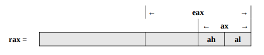
As shown in the diagram, the first four registers, rax, rbx, rcx, and rdx also allow the bits 8-15 to be accessed with the ah, bh, ch, and dh register names.
The ability to access portions of the register means that, if the quadword rax register is set to 50,000,000,00010 (fifty billion), the rax register would contain the following value in hex.
rax = 0000 000B A43B 7400
If a subsequent operation sets the word ax register to 50,00010 in decimal (fifty thousand, which is C35016 in hex), the rax register would contain the following value in hex.
rax = 0000 000B A43B C350
In this case, when the lower 16-bit ax portion of the 64-bit rax register is set, the upper 48-bits are unaffected. Note the change in ax (from 740016 (hex) to C35016 (hex)).
If a subsequent operation sets the byte sized al register to 5010 in decimal (fifty, which is 3216 in hex), the rax register would contain the following value in hex.
rax = 0000 000B A43B C332
When the lower 8-bit al portion of the 64-bit rax register is set, the upper 56-bits are unaffected. Note the change in al (from 5016 to 3216).
Stack Pointer Register (RSP)
One of the CPU registers, rsp, is used to point to the current top of the stack. The rsp register should not be used for data or other uses.
Base Pointer Register (RBP)
One the CPU registers, rbp, is used as a base pointer during function calls. The rbp register should not be used for data or other uses.
Instruction Pointer Register (RIP)
In addition to the GPRs, there is a special register, rip, which is used by the CPU to point to the next instruction to be executed. Specifically, since the rip points to the next instruction, that means the instruction being pointed to by rip, and shown in the debugger, has not yet been executed.
Flag Register (rFlags)
The flag register, rFlags is used for status and CPU control information. The rFlags register is updated by the CPU after each instruction and not directly accessible by programs. This register stores status information about the instruction that was just executed.
The following table shows some of the status bits in the flag register.
| Name | Symbol | Bit | Use |
| Carry | CF | 0 | Used to indicate if the previous operation resulted in a carry. |
| Parity | PF | 2 | Used to indicate if the last byte has an even number of 1's (i.e., even parity). |
| Adjust | AF | 4 | Used to support Binary Coded Decimal operations. |
| Zero | ZF | 6 | Used to indicate if the previous operation resulted in a zero result. |
| Sign | SF | 7 | Used to indicate if the result of the previous operation resulted in a 1 in the most significant bit (indicating negative in the context of signed data). |
| Direction | DF | 10 | Used to specify the direction (increment or decrement) for some string operations. |
| Overflow | OF | 11 | Used to indicate if the previous operation resulted in a overflow. |
XMM Registers
There are a set of dedicated registers used to support 64-bit and 32-bit floating-point operations and Single Instructions Multiple Data (SIMD) instructions.
Cache Memory
Cache Memory is a small subset of the primary storage or RAM located in the CPU chip. If a memory location is accessed, a copy of the value is placed in the cache. Subsequent accesses to that memory location that occur in quick succession are retrieved from the cache location (internal to the CPU chip). A memory read involves sending the address via the bus to the memory controller, which will obtain the value at the requested memory location, and send it back through the bust. Comparatively, if a value is cache, it would be much faster to access that value.
A cache hit occurs when the requested data can be found in a cache, while cache miss occurs when it cannot. Cache hits are served by reading data from the cache, which is faster than reading from main memory. The more requests that can be served from cache, the faster the system will typically perform. Successive generations of CPU chips have increases cache memory and improved cache mapping strategies in order to improve overall performance.
A block diagram of a typical CPU chip configuration is as follows:
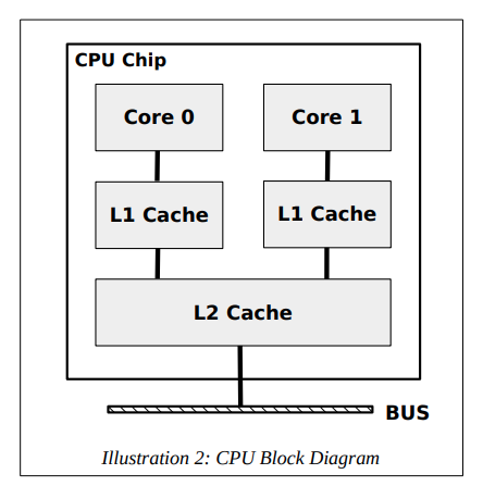
Most chip designs typically include an L1 cache per core and a shared L2 cache. Many of the newer CPU chips will have an additional L3 cache.
As can be noted from the diagram, all memory accesses travel through each level of cache. As such, there is a potential for multiple, duplicate copies of the value (CPU register, L1 cache, L2 cache, and main memory). This complication is managed by the CPU and is not something the programmer can change.
Main Memory
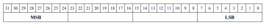
Memory can be viewed as a series of bytes, one after another. That is, memory is byte addressable. This means each memory address holds one byte of information. To store a double-word, four bytes are required which use four memory addresses.
Additionally, architecture is little-endian. This means that the Least Significant Byte (LSB) is stored in the lowest memory address. The Most Significant Byte (MSB) is stored in the highest memory location.
For a double-word (32-bits), the MSB and LSB are allocated as shown below.
For example, assuming the value of 5,000,000 (004C4B40 in hex) is to be placed in a double-word variable named var1.
For a little-endian, the memory picture would be as follows:
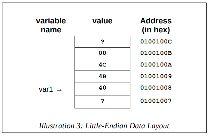
Based on the little-endian architecture, the LSB is stored in the lowest memory address and the MSB is stored in the highest memory location.
CPU Instruction Cycle
The instruction cycle, also known as the fetch-decode-execute cycle, is the process through which the CPU executes instructions.
But first let's first get familiar with some things:
Program Counter:
- The PC is a register that holds the memory address of the next instruction to be fetched and executed by the CPU.
- It is a general term often used in the context of various computer architectures.
- The PC is incremented automatically after each instruction fetch, unless modified by a control transfer instruction like a jump, call, or branch.
- The size of the increment depends on the instruction set architecture. For instance, in a
32-bitsystem, the increment would be4 bytes. - For example, suppose the content of PC is
8000H. Which means that the processor wants to fetch the instruction byte on 8000H. After fetching the byte at8000H, the PC automatically increments by one (1). In this way the processor becomes ready to fetch the next byte of the instruction or to fetch the next opcode.
Instruction Pointer:
- This is a specific term often used in the context of certain architectures, particularly the x86 architecture, to refer to the register that serves the same purpose as the Program Counter.
- In the x86 architecture, the register that holds the address of the next instruction is called the Instruction Pointer (IP) in 16-bit mode and the Extended Instruction Pointer (EIP) in 32-bit mode. In 64-bit mode, it is referred to as the RIP (64-bit Instruction Pointer).
- IP: Instruction Pointer for 16-bit mode, holding the 16-bit address of the next instruction.
- EIP: Extended Instruction Pointer for 32-bit mode, holding the 32-bit address of the next instruction.
- RIP: 64-bit Instruction Pointer for 64-bit mode, holding the 64-bit address of the next instruction.
mov eax, 1    ; Instruction at address 0x00400000
add eax, 2    ; Instruction at address 0x00400004
jmp 0x00400010; Instruction at address 0x00400008
- Initially, the EIP (Extended Instruction Pointer) is set to
0x00400000. - The
mov eax, 1instruction is fetched from this address, and EIP is incremented to0x00400004. - The
add eax, 2instruction is fetched, and EIP is incremented to0x00400008. - The
jmp 0x00400010instruction is fetched, and EIP is updated to0x00400010,causing a jump to the new address.
Instruction Register:
It holds the instruction currently being executed or decoded, serving as a temporary storage for the fetched instruction before it is processed.
- Temporary Storage: The IR temporarily holds the binary-encoded instruction fetched from memory before it is decoded and executed by the CPU.
- Instruction Decoding: Once an instruction is loaded into the IR, the control unit decodes it to understand the operation to be performed and the operands involved.
- Control Signal Generation: The IR aids the control unit in generating the appropriate control signals needed for executing the instruction.
The CPU executes instructions in a sequential manner, following the fetch-decode-execute cycle:
- Fetch: The control unit retrieves instructions from the computer's memory, using the Program Counter to determine the next instruction's location.
- The Program Counter (PC) holds the address of the next instruction.
- The control unit places this address on the address bus.
- The instruction is fetched from memory into the Instruction Register (IR).
- Decode: The fetched instructions are decoded by the Control Unit, determining the type of operation to be performed and the associated operands.
- The control unit decodes the instruction in the IR.
- It determines the operation to be performed and identifies the operands involved.
- Control signals are generated to direct other components of the CPU.
- Execute: The ALU executes the decoded instruction using the operands. This could involve arithmetic or logical operations, data transfer, or control operations like branching.
The results of the execution are stored in the specified destination, such as a register or a memory location. - Write Back Data (optional): If necessary, the results of the execution are written back to the appropriate location, such as updating a register or writing data to memory.
Detailed Example: Execution of an ADD Instruction
Let's consider an ADD instruction that adds the contents of two registers and stores the result in one of them. Here's step-by-step explanation:
1 Instruction: ADD R1, R2 (where R1 and R2 are registers):
- Purpose: Add the contents of register R2 to register R1 and store the result in R1.
2 Fetch:
- The PC (Program Counter) points to the address of the ADD instruction.
- The control unit fetches the instruction from memory into the IR (Instruction Register).
- The PC (Program Counter) is incremented to point to the next instruction.
3 Decode:
- The instruction decoder in the control unit interprets the ADD instruction.
- It identifies the operation (addition) and the operands (R1 and R2).
4 Execute:
- The control unit sends control signals to the ALU and registers.
- The contents of R2 are retrieved and sent to the ALU.
- The ALU adds the contents of R1 and R2.
- The result is stored back in R1.
5 Write Back:
- The result (sum of R1 and R2) is written back to R1.
- The status flags are updated based on the result (e.g., Zero Flag if the result is zero).
Registers
As we all know, registers are a part of the CPU. They are small in size however extremely fast to access. There are different kinds of registers in x86-64.
1 General-Purpose Registers (GPRs)
- The x86_64 architecture features a set of 16 general-purpose registers, each 64 bits wide.
- These registers are denoted by names such as RAX, RBX, RCX, RDX, RSI, RDI, RBP, RSP, R8-R15.
| Register (64 bit) | Lower byte (8-bit) | Lower word (8-bit) | Lower dword (32-bit) |
| rax | al | ax | eax |
| rbx | bl | bx | ebx |
| rcx | cl | cx | ecx |
| rdx | dl | dx | edx |
| rsp | spl | sp | esp |
| rsi | sil | si | esi |
| rdi | dil | di | edi |
| rbp | bpl | bp | ebp |
| r8 | r8b | r8w | r8d |
| r9 | r9b | r9w | r9d |
| r10 | r10b | r10w | r10d |
| r11 | r11b | r11w | r11d |
| r12 | r12b | r12w | r12d |
| r13 | r13b | r13w | r13d |
| r14 | r14b | r14w | r14d |
| r15 | r15b | r15w | r15d |
2 Program Counter (PC) || Instruction Pointer (IP):
- The term “Program Counter” and “Instruction Pointer” are often used interchangeably. In x86_64 architecture, the term
Instruction Pointeris typically used to refer to this register, while in other architectures or contexts,Program Countermight be more commonly used. - The Program Counter (PC) register holds the memory address of the next instruction to be executed.
- As instructions are fetched and executed, the PC is updated to point to the next instruction in sequence, enabling the CPU to proceed with program execution.
3 Flags Register (RFLAGS):
- The Flags Register, often referred to as RFLAGS in x86_64 architecture, stores status flags that indicate the outcome of arithmetic and logical operations.
- These flags include the carry flag, zero flag, sign flag, overflow flag, and many others, providing valuable information about the result of operations.
Memory Layout
The general memory layout for a program is as shown:
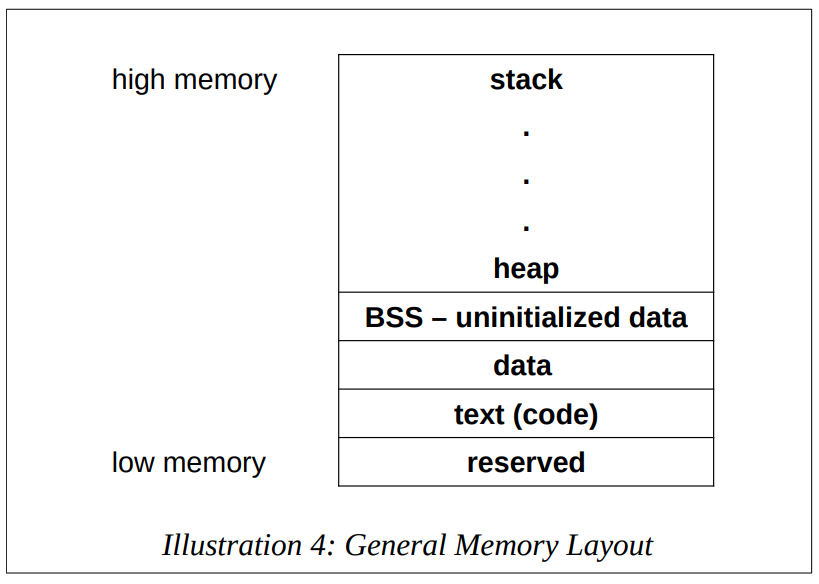
The reserved section is not available for user programs. The text (or code) section is where the machine language (i.e., the 1's and 0's that represents the code) is stored. The data section is where the initialized data is stored. This includes declared variables that have been provided an initial value at assemble-time. The uninitialized data section, typically called BSS section, is where declared variables that have not been provided an initial value are stored. If accessed before being set, the value will not be meaningful. The heap is where dynamically allocated data will be stored (if requested). The stack starts in high memory and grows downward.
Memory Hierarchy
In General terms, faster memory is more expensive and slower memory blocks are less expensive. The CPU registers are small, fast, and expensive. Secondary storage devices such as disk drives and Solid State Drives (SSD's) are larger, slower, and less expensive.
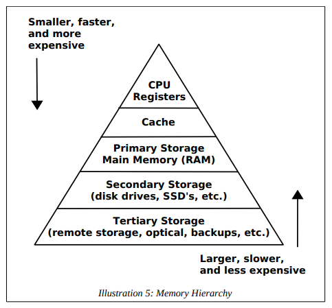
With the top of the triangle represents the fastest, smallest, and most expensive memory. As we move down levels, the memory becomes slower, larger, and less expensive.
CPU Clocks
The clock sets the rate at which CPU changes state. The faster the clock, the more the CPU can do in a given amount of time.
The CPU clock, also known as the system clock or processor clock, is a fundamental component of a computer's architecture. It generates electrical pulses at a constant rate, which synchronizes the operations of the CPU and other components of the computer system. The CPU clock determines the speed at which instructions are executed and data is processed by the CPU.
The speed of a computer processor, or CPU, is determined by the Clock Cycle, which is the amount of time between two pulses of an oscillator. Generally speaking, the higher number of pulses per second, the faster the computer processor will be able to process information. The clock speed is measured in Hz, typically either megahertz (MHz) or gigahertz (GHz).
- The clock/oscillator is located in a chip on the motherboard ('chipset), not inside the processor.
How the CPU Clock Works:
- Clock Signal Generation: The CPU clock generates a series of electrical pulses, known as clock cycles or ticks, at a constant frequency.
- Synchronization: All operations within the CPU, including instruction execution and data processing, are synchronized to the CPU clock. Each clock cycle represents a fixed unit of time.
- Instruction Execution: The CPU executes instructions in discrete steps, with each step occurring during a single clock cycle. This includes fetching instructions from memory, decoding them, executing them, and storing the results.
CPU Clock Speed
The speed of the CPU clock is measured in hertz (Hz) and represents the number of clock cycles per second. Common units of CPU clock speed include:
- 1 Hertz: 1 signal in 1 second.
- 1 Kilohertz: 1000 signals in 1 second.
- 1 Megahertz (MHz): Millions of clock cycles per second (10^6 = 1,000,000 signals in 1 second).
- 1 Gigahertz (GHz): Billions of clock cycles per second (10^9 = 1,000,000,000 signals per seconds)
For example, a CPU with a clock speed of 2.5 GHz executes 2.5 billion clock cycles per second.
Relationship with Memory Access
The CPU clock determines the rate at which the CPU can access data from memory. In a 32-bit system, for instance, the CPU can read 32 bits (4 bytes) of data from memory in a single clock cycle.

Leave a comment
Your email address will not be published. Required fields are marked *