In real mode we can read data directly from the disk without relying on the BIOS interrupts. This can be achieved by interacting directly with the ATA/ATAPI controller using x86 assembly language in real mode.
1 What is ATA/ATAPI?
ATA (Advanced Technology Attachment), also known as IDE (Integrated Drive Electronics), is a standard interface for connecting storage devices like hard drives and SSDs. ATAPI (ATA Packet Interface) extends ATA to support optical drives and other storage devices. In real mode, we typically interact with ATA using PIO (Programmed Input/Output) mode.
The communication with storage devices (such as hard drives and CD-ROM drives) is achieved through a set of I/O ports. These ports are used to send commands, read status, and transfer data between the CPU and the storage device.
1.2 ATA/ATAPI I/O Ports
Here are the primary I/O ports used for interacting with ATA/ATAPI devices:
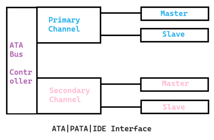
Primary and Secondary Channels
Typically, a computer has two ATA channels: primary and secondary. Each channel can connect to two devices (master and slave). Each channel has a set of I/O ports.
- Primary Channel: 0x1F0 - 0x1F7 (Data port through Command port), and 0x3F6 (Control port).
- Secondary Channel: 0x170 - 0x177 (Data port through Command port), and 0x376 (Control port).
1.3 Primary Channel Ports
| Port | Register | Description |
|---|---|---|
| 0x1F0 | Data Register | Used to read/write data (16 bits) |
| 0x1F1 | Error Register | Provides error codes (read) / Features Register (write) |
| 0x1F2 | Sector Count Register | Number of sectors to read/write |
| 0x1F3 | Sector Number Register | Starting sector number (LBA low byte) |
| 0x1F4 | Cylinder Low Register | Cylinder number low byte (LBA mid byte) |
| 0x1F5 | Cylinder High Register | Cylinder number high byte (LBA high byte) |
| 0x1F6 | Drive/Head Register | Selects the drive and head |
| 0x1F7 | Status Register (read) | Status of the device |
| Command Register (write) | Issues commands to the device | |
| 0x3F6 | Alternate Status Register | Duplicate status register (read) / Device Control Register (write) |
1.4 Secondary Channel Ports
| Port | Register | Description |
|---|---|---|
| 0x170 | Data Register | Used to read/write data (16 bits) |
| 0x171 | Error Register | Provides error codes (read) / Features Register (write) |
| 0x172 | Sector Count Register | Number of sectors to read/write |
| 0x173 | Sector Number Register | Starting sector number (LBA low byte) |
| 0x174 | Cylinder Low Register | Cylinder number low byte (LBA mid byte) |
| 0x175 | Cylinder High Register | Cylinder number high byte (LBA high byte) |
| 0x176 | Drive/Head Register | Selects the drive and head |
| 0x177 | Status Register (read) | Status of the device |
| Command Register (write) | Issues commands to the device | |
| 0x376 | Alternate Status Register | Duplicate status register (read) / Device Control Register (write) |
1.5 Common ATA Commands
- 0x20: Read Sectors (with retry)
- 0x21: Read Sectors (without retry)
- 0x30: Write Sectors (with retry)
- 0x31: Write Sectors (without retry)
- 0xE7: Flush Cache
- 0xEC: Identify Device
2 Reading Disk Using ATA PIO Mode
Here's a step-by-step guide to read sectors from the disk using ATA PIO mode in x86 assembly language.
Step 1: Initialize the Disk Controller
Before reading from the disk, you need to initialize the ATA controller.
Step 2: Send Commands to Read Sectors
To read from the disk, you need to send appropriate commands to the ATA controller. This involves setting the drive/head, cylinder, sector, and issuing the read command.
Step 3: Load Data into Memory
Once the controller is set up, you read the data from the disk into memory.
What is ATA?
ATA is a disk drive interface standard developed by the American National Standards Institute (ANSI). It is primarily used for connecting storage devices to a computer's motherboard using standardized protocols, commands, and electrical connections. Over time, ATA has undergone various iterations, improving performance, capacity, and features.
It is also known as Integrated Drive Electronics (IDE).
After the introduction of SATA, the earlier ATA were known as the PATA.
So ATA = PATA = IDE
ATA vs. SATA
Serial ATA (SATA) is the successor to the original ATA standard. While ATA (or Parallel ATA, PATA) uses a parallel signaling method, SATA employs serial signaling, offering several advantages:
- Higher Data Transfer Rates: SATA supports much higher data transfer rates, starting at 150 MB/s (SATA I) and going up to 600 MB/s (SATA III).
- Improved Cable Management: SATA cables are thinner and longer than ATA cables, allowing for better airflow and easier cable management inside the computer case.
- Hot Swapping: SATA supports hot swapping, allowing drives to be connected and disconnected without powering down the system.
ATA Interface
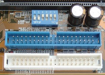
As you can see in the picture above, there are two PATA ports one in blue and other in white. One of them is called as the Primary port while the other as Secondary port. Each Port is capable of connecting two devices, such that this motherboard able to connect four devices with the PATA interface. Those four devices can be hard disk, floppy disk, cd-drive and any other secondary drive.
+------------------------------------+
|                                    |
|            CPU/Memory              |
|                                    |
+------------------------------------+
                |
                | I/O Instructions (IN/OUT)
                |
                v
+------------------------------------+
|                                    |
|      ATA Interface (Motherboard)   |
|                                    |
|  +----------------------------+    |
|  | Primary Channel            |    |
|  |                            |    |
|  | +------------------------+ |    |
|  | | Primary I/O Registers  | |    |
|  | |                        | |    |
|  | | Data Register (0x1F0)  | |    |
|  | | Error Register (0x1F1) | |    |
|  | | Sector Count (0x1F2)   | |    |
|  | | LBA Low (0x1F3)        | |    |
|  | | LBA Mid (0x1F4)        | |    |
|  | | LBA High (0x1F5)       | |    |
|  | | Device/Head (0x1F6)    | |    |
|  | | Command (0x1F7)        | |    |
|  | | Status (0x1F7)         | |    |
|  | +------------------------+ |    |
|  |                            |    |
|  +----------------------------+    |
|                                    |
|  +----------------------------+    |
|  | Secondary Channel          |    |
|  |                            |    |
|  | +------------------------+ |    |
|  | | Secondary I/O Registers| |    |
|  | |                        | |    |
|  | | Data Register (0x170)  | |    |
|  | | Error Register (0x171) | |    |
|  | | Sector Count (0x172)   | |    |
|  | | LBA Low (0x173)        | |    |
|  | | LBA Mid (0x174)        | |    |
|  | | LBA High (0x175)       | |    |
|  | | Device/Head (0x176)    | |    |
|  | | Command (0x177)        | |    |
|  | | Status (0x177)         | |    |
|  | +------------------------+ |    |
|  |                            |    |
|  +----------------------------+    |
|                                    |
+------------------------------------+
                |
                | ATA Interface (Ribbon Cable)
                |
                v
+------------------------------------+
|                                    |
|          ATA Device(s)             |
|                                    |
|  +----------------------------+    |
|  | Device 0 (Master)          |    |
|  |                            |    |
|  | +------------------------+ |    |
|  | | Integrated Controller  | |    |
|  | |                        | |    |
|  | | Data, Command, Status  | |    |
|  | +------------------------+ |    |
|  |                            |    |
|  +----------------------------+    |
|                                    |
|  +----------------------------+    |
|  | Device 1 (Slave)           |    |
|  |                            |    |
|  | +------------------------+ |    |
|  | | Integrated Controller  | |    |
|  | |                        | |    |
|  | | Data, Command, Status  | |    |
|  | +------------------------+ |    |
|  |                            |    |
|  +----------------------------+    |
|                                    |
+------------------------------------+
- The motherboard has an ATA interface that consists of connectors (typically 40-pin or 80-pin ribbon cables) and a small set of I/O ports that facilitate communication between the CPU/memory and the ATA drives.
- The ATA interface on the motherboard includes the primary and secondary channels with their respective I/O port addresses (e.g., 0x1F0-0x1F7 for the primary channel and 0x170-0x177 for the secondary channel).
Channels:
A "channel" refers to a pathway through which data is transmitted between the computer's motherboard (specifically the ATA controller) and the connected storage devices (such as hard drives or optical drives).
- Primary Channel: Allows connection of up to two devices (one master and one slave).
- Secondary Channel: Adds capacity for another two devices (one master and one slave).
- Total Devices: By using both channels, a system can support up to four ATA devices simultaneously.
Primary Channels
- I/O Port Addresses: Typically uses port addresses ranging from
0x1F0 to 0x1F7. - Devices: Supports up to two devices (master and slave).
- Primary I/O Registers: These registers are used to issue commands, read/write data, and check the status of the device.
- Data Register (0x1F0): Used for data transfer.
- Error Register (0x1F1): Provides error information.
- Sector Count Register (0x1F2): Specifies the number of sectors to read/write.
- LBA Low (0x1F3), LBA Mid (0x1F4), LBA High (0x1F5): Used to specify the Logical Block Address (LBA).
- Device/Head Register (0x1F6): Selects the device (master/slave) and the head.
- Command Register (0x1F7): Used to issue commands to the device.
- Status Register (0x1F7): Provides the status of the device.
Secondary Channel:
- I/O Port Addresses: Typically uses port addresses ranging from
0x170 to 0x177. - Devices: Supports up to two devices (master and slave)
- Similar to the primary channel, but typically uses I/O port addresses from 0x170 to 0x177.
Example of Device Configuration:
Imagine a typical desktop computer setup:
- Primary Channel:
- Master Device: 500GB HDD
- Slave Device: 250GB HDD
- Secondary Channel:
- Master Device: DVD-RW Drive
- Slave Device: CD-RW Drive
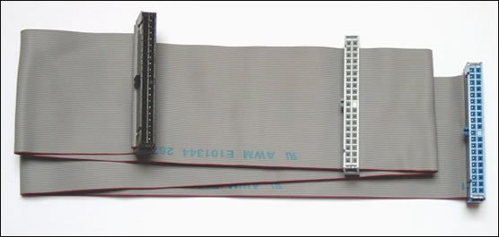
ATA Interface (Ribbon Cable):
- Connects the ATA controller to the ATA devices (hard drives, optical drives, etc.).
- It has three connectors
- One for the motherboard.
- One for the master device.
- One for the slave device.

+---------------------------------------------+
| Motherboard Connector                       |
| (usually blue)                              |
+---------------------------------------------+
                    |    |
                    |    |
                    |    |
                    |    |
+-------------------+----+--------------------+
| Slave Device Connector (middle)             |
| (usually grey)                              |
+---------------------------------------------+
                    |    |
                    |    |
                    |    |
                    |    |
+---------------------------------------------+
| Master Device Connector (end)               |
| (usually black)                             |
+---------------------------------------------+
ATA Device(s):
- Device 0 (Master) and Device 1 (Slave): Each device has its own internal registers for managing data, commands, and status.
ATA Architecture
ATA is characterized by a parallel bus architecture, which allows multiple bits of data to be transferred simultaneously. Key components of the ATA architecture include:
- Controller: The controller is integrated into the storage device, which is why it's called Integrated Drive Electronics (IDE). It manages communication between the ATA devices and the computer.
- It has two main channels: primary and secondary, each with its own set of I/O registers.
- Data Bus: A 16-bit wide parallel data bus that transfers data between the storage device and the motherboard.
- I/O Ports: Specific ports are used for sending commands, receiving status information, and transferring data.
- Registers: Several registers are used to control the device, send commands, and handle data. Key registers include the Data Register, Error Register, Sector Count Register, Sector Number Register, Cylinder Registers, and Drive/Head Register.
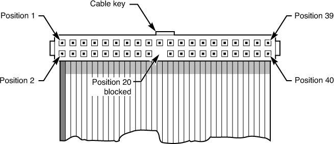
ATA Interface Signals and Pins:
        +-------------------------------------------------------------+
Pin 1 ->| o o o o o o o o o o o o o o o o o o o o o o o o o o o o o o |<- Pin 40
Pin 2 ->| o o o o o o o o o o o o o o o o o o o o o o o o o o o o o o |<- Pin 39
        +-------------------------------------------------------------+
The ATA interface typically uses a 40-pin ribbon cable. The key signals include:
- Data Signals (D0-D15): A 16-bit data bus for transferring data between the device and the host.
- Address Signals (A0-A2): Used to select registers within the device.
- Control Signals:
- CS0/CS1: Chip select lines to select the command block or control block registers.
- DIOR- (I/O Read): Indicates a read operation from the host.
- DIOW- (I/O Write): Indicates a write operation from the host.
- IOR- (I/O Read): Combined with DIOR- in ATA mode.
- IOW- (I/O Write): Combined with DIOW- in ATA mode.
- INTRQ: Interrupt request signal.
- PDIAG-: Passed diagnostics signal.
- DASP-: Device active or slave present signal.
| Pin | Signal Name | Description |
|---|---|---|
| 1 | RESET- | Host reset signal |
| 2 | GND | Ground |
| 3 | DD7 | Data bit 7 |
| 4 | DD8 | Data bit 8 |
| 5 | DD6 | Data bit 6 |
| 6 | DD9 | Data bit 9 |
| 7 | DD5 | Data bit 5 |
| 8 | DD10 | Data bit 10 |
| 9 | DD4 | Data bit 4 |
| 10 | DD11 | Data bit 11 |
| 11 | DD3 | Data bit 3 |
| 12 | DD12 | Data bit 12 |
| 13 | DD2 | Data bit 2 |
| 14 | DD13 | Data bit 13 |
| 15 | DD1 | Data bit 1 |
| 16 | DD14 | Data bit 14 |
| 17 | DD0 | Data bit 0 |
| 18 | DD15 | Data bit 15 |
| 19 | GND | Ground |
| 20 | (NC) | Not connected / key pin |
| 21 | DMARQ | DMA request |
| 22 | GND | Ground |
| 23 | DIOW- | I/O write strobe |
| 24 | GND | Ground |
| 25 | DIOR- | I/O read strobe |
| 26 | GND | Ground |
| 27 | IORDY | I/O channel ready |
| 28 | CSEL | Cable select |
| 29 | DMACK- | DMA acknowledge |
| 30 | GND | Ground |
| 31 | INTRQ | Interrupt request |
| 32 | IOCS16- | 16-bit I/O |
| 33 | DA1 | Address bit 1 |
| 34 | PDIAG- | Passed diagnostics |
| 35 | DA0 | Address bit 0 |
| 36 | DA2 | Address bit 2 |
| 37 | CS1FX- | Chip select 1 |
| 38 | CS3FX- | Chip select 3 |
| 39 | DASP- | Device active or slave present |
| 40 | GND | Ground |
Explanation of Key Pins
- Data Pins (DD0 - DD15):
- These 16 pins are used for the bidirectional data bus to transfer data between the drive and the host system.
- Ground Pins (GND):
- Several pins are dedicated to ground connections, providing a common return path for electrical current and minimizing noise.
- Control Signals:
- RESET- (Pin 1): Used to reset the drive.
- DMARQ (Pin 21): Used by the drive to request a DMA transfer.
- DIOW- (Pin 23): Indicates that the host is writing data to the drive.
- DIOR- (Pin 25): Indicates that the host is reading data from the drive.
- IORDY (Pin 27): Used by the drive to signal that it is ready to transfer data.
- CSEL (Pin 28): Determines the drive configuration (master/slave) based on the cable.
- DMACK- (Pin 29): Acknowledge signal from the host for DMA transfers.
- INTRQ (Pin 31): Used by the drive to signal an interrupt request.
- IOCS16- (Pin 32): Indicates that 16-bit data transfers are supported.
- CS1FX- and CS3FX- (Pins 37, 38): Chip select signals for accessing the command and control blocks.
- DASP- (Pin 39): Indicates that the drive is active or that a slave drive is present.
- Address Pins (DA0 - DA2):
- These pins are used to select specific registers within the drive's internal architecture.
- Key Pin (NC):
- Pin 20 is typically not connected and serves as a key pin to ensure proper orientation of the connector.
ATA Registers:
The ATA standard defines several registers that are used to send commands to the device, read status, and transfer data. These registers are typically accessed through specific I/O ports. The ATA (Advanced Technology Attachment) registers are situated within the I/O (Input/Output) address space of the computer system. They are accessed using specific I/O port addresses, which are standardized for ATA devices.
Understanding I/O Port Addresses:
- I/O Port Addressing: In computer architecture, I/O ports are numbered locations in memory where devices (such as ATA controllers) communicate with the CPU. These addresses are typically in a separate address space from main memory.
- Access Methods: To interact with ATA registers, the CPU uses special instructions (
INfor reading andOUTfor writing) to access data at these specific I/O port addresses.
-: Primary ATA Channel I/O Port Addresses :-
- Data Register:
0x1F0 - Error Register (Read) / Features Register (Write):
0x1F1 - Sector Count Register:
0x1F2 - LBA Low Register:
0x1F3 - LBA Mid Register:
0x1F4 - LBA High Register:
0x1F5 - Device/Head Register:
0x1F6 - Command Register (Write) / Status Register (Read):
0x1F7 - Alternate Status Register (Read) / Device Control Register (Write):
0x3F6
-: Secondary ATA Channel I/O Port Addresses :-
- Data Register:
0x170 - Error Register (Read) / Features Register (Write):
0x171 - Sector Count Register:
0x172 - LBA Low Register:
0x173 - LBA Mid Register:
0x174 - LBA High Register:
0x175 - Device/Head Register:
0x176 - Command Register (Write) / Status Register (Read):
0x177 - Alternate Status Register (Read) / Device Control Register (Write):
0x376
Detailed Description of ATA Registers:
1 Data Register (0x1F0 / 0x170):
- Function: Used to read and write data to/from the drive.
- Data Size: 16-bit.
2 Error Register (0x1F1 / 0x171) [Read]:
- Function: Contains status information about errors that occurred during the previous command.
- Bits:
0: Address mark not found.1: Track zero not found.2: Command aborted.3: Media change requested.4: ID not found.5: Media changed.6: Uncorrectable data error.7: Bad block detected.
3 Features Register (0x1F1 / 0x171) [Write]:
- Function: Used to specify features to be enabled or options to be set for the command being issued.
4 Sector Count Register (0x1F2 / 0x172):
- Function: Specifies the number of sectors to read or write.
5 LBA Low Register (0x1F3 / 0x173):
- Function: Specifies the low-order 8 bits of the Logical Block Address (LBA).
6 LBA Mid Register (0x1F4 / 0x174):
- Function: Specifies the middle-order 8 bits of the Logical Block Address (LBA).
7 LBA High Register (0x1F5 / 0x175):
- Function: Specifies the high-order 8 bits of the Logical Block Address (LBA).
8 Device/Head Register (0x1F6 / 0x176):
- Function: Selects the target drive and specifies the 4 highest bits of the Logical Block Address (LBA).
- Bits:
7: 1 (always set).6: LBA mode (0 for CHS, 1 for LBA).5: Drive (0 for master, 1 for slave).4-0: Bits 24-27 of LBA.
9 Command Register (0x1F7 / 0x177) [Write]:
- Function: Used to issue commands to the drive (e.g., read, write, identify).
- Common Commands:
0x20: Read Sectors.0x30: Write Sectors.0xEC: Identify Drive.
10 Status Register (0x1F7 / 0x177) [Read]:
- Function: Provides the current status of the drive.
- Bits:
0: Error.1: Index (not used).2: Corrected data (not used).3: Data request.4: Service request (overlapped feature).5: Drive fault.6: Ready.7: Busy.
| Bit | Name | Description |
|---|---|---|
| 7 | BSY | Busy: The device is busy with an operation. |
| 6 | DRDY | Device Ready: The device is ready to accept commands. |
| 5 | DF/SE | Device Fault or Stream Error: An error has occurred. |
| 4 | DSC | Device Seek Complete: The device has completed a seek. |
| 3 | DRQ | Data Request: The device is ready to transfer data. |
| 2 | CORR | Corrected Data: Data has been corrected (obsolete). |
| 1 | IDX | Index: Set once per disk revolution (obsolete). |
| 0 | ERR | Error: An error occurred with the previous command. |
- Bit 7 (BSY - Busy):
- Indicates that the device is busy with an operation and cannot accept new commands.
1: Device is busy.0: Device is not busy.
- Indicates that the device is busy with an operation and cannot accept new commands.
- Bit 6 (DRDY - Device Ready):
- Indicates that the device is ready to accept commands.
1: Device is ready.0: Device is not ready.
- Indicates that the device is ready to accept commands.
- Bit 5 (DF/SE - Device Fault or Stream Error):
- Indicates a device fault or stream error.
1: Device fault or stream error detected.0: No device fault or stream error.
- Indicates a device fault or stream error.
- Bit 4 (DSC - Device Seek Complete):
- Indicates that a seek operation has been completed.
1: Seek operation complete.0: Seek operation not complete.
- Indicates that a seek operation has been completed.
- Bit 3 (DRQ - Data Request):
- Indicates that the device is ready to transfer data (read or write).
1: Device is ready to transfer data.0: Device is not ready to transfer data.
- Indicates that the device is ready to transfer data (read or write).
- Bit 2 (CORR - Corrected Data):
- Indicates that the data has been corrected (this bit is obsolete in modern devices).
1: Data corrected.0: No correction.
- Indicates that the data has been corrected (this bit is obsolete in modern devices).
- Bit 1 (IDX - Index):
- Set once per disk revolution (this bit is obsolete in modern devices).
1: Index set.0: Index not set.
- Set once per disk revolution (this bit is obsolete in modern devices).
- Bit 0 (ERR - Error):
- Indicates that an error occurred with the previous command.
1: Error occurred.0: No error.
- Indicates that an error occurred with the previous command.
11 Alternate Status Register (0x3F6 / 0x376) [Read]:
- Function: Provides the same information as the status register but does not clear interrupts or the status bits.
12 Device Control Register (0x3F6 / 0x376) [Write]:
- Function: Used to control the drive’s interrupt and reset features.
- Bits:
0-1: Reserved.2: Software reset.3: Interrupt disable.4-7: Reserved.
Communication Process
The communication between the CPU and the ATA device involves several steps, which can be broadly categorized into command issuance, data transfer, and status checking.
- Command Issuance:
- The CPU sends commands to the storage device by writing to the Command Register.
- Commands are typically accompanied by parameters written to other registers (e.g., sector number, cylinder number, etc.).
- Data Transfer:
- Data is transferred between the CPU and the storage device via the Data Register.
- ATA supports two primary modes for data transfer: Programmed Input/Output (PIO) and Direct Memory Access (DMA).
- Status Checking:
- The CPU reads the Status Register to check the status of the device and ensure the completion of operations.
- The Status Register provides information about errors, readiness, and busy states.
ATA Command Set
The ATA command set defines a series of commands that the operating system can use to interact with the storage device. Some essential ATA commands include:
- IDENTIFY DEVICE (0xEC): Retrieves detailed information about the storage device, such as its capabilities and specifications.
- READ SECTORS (0x20): Reads data from specified sectors on the storage device.
- WRITE SECTORS (0x30): Writes data to specified sectors on the storage device.
- SEEK (0x70): Moves the read/write head to a specified cylinder.
Data Transfer Modes (Protocols)
ATA supports two primary data transfer modes: Programmed Input/Output (PIO) and Direct Memory Access (DMA).
PIO Mode: In PIO mode, the CPU directly controls the data transfer between the storage device and memory. The CPU reads and writes data to the device's data register. This mode is simpler but can be slower due to the CPU’s involvement in the transfer process.
- PIO Data Transfer Steps:
- The CPU sends a READ or WRITE command to the device.
- The CPU waits for the device to signal readiness.
- The CPU reads or writes data to/from the device’s data register.
- The CPU handles any interrupts generated by the device.
DMA Mode: In DMA mode, data is transferred directly between the storage device and memory, bypassing the CPU. This mode is faster and more efficient, especially for large data transfers, as it reduces CPU involvement.
- DMA Data Transfer Steps:
- The CPU sets up the DMA controller with the source and destination addresses and the amount of data to transfer.
- The CPU sends a DMA READ or WRITE command to the device.
- The DMA controller manages the data transfer between the device and memory.
- The device generates an interrupt upon completion, which the CPU handles.
Detect Device:
Identifying ATA (Advanced Technology Attachment) devices, such as hard drives and optical drives, involves querying the devices for their identifying information using specific commands and registers.
It's like checking which device is connected to the channels. Since we have two channel and each channel support two devices. Thus we need to check for all the four devices.
Using the Identify Device Command:
The primary method to identify ATA devices is by sending the Identify Device command (0xEC) to the device and then reading the data from specific registers. Here are the steps involved:
1 Select the Device:
As we know that ATA devices are usually connected to either the primary of primary or secondary ATA bus (channel), and each bus can have a master and a slave device.
Use the OUT instruction to select the ATA device (master or slave) and specify LBA mode if needed. This is done by writing to the Device/Head register (0x1F6 for master, 0x170 for slave).
; Example: Select Master device and LBA mode

; 0x1F6  = Device/Head Register for primary ATA bus

; 0x170 =  Device/Head Register for seconary ATA bus

mov dx, 0x1F6   ; Port address of Device/Head register
mov al, 0xA0    ; Select Master device, bit 6 set for LBA mode
				; 0xA0 for master device
				; 0xB0 for slave device
out dx, al      ; Send command to Device/Head register
2 Issue Identify Command:
Write the Identify Device command (0xEC) to the Command/Status register (0x1F7 for the primary bus (channel), 0x177 for the secondary bus (channel)) to request the identification data from the ATA device.
The command register is also known as status register:
- Writing to the Port: When you write to the port, it is interpreted as a command.
- Reading from the Port: When you read from the port, it is interpreted as a status.
The command register is used to send commands to the ATA device. Common commands include:
- 0xEC: Identify Device
- 0x20: Read Sectors
- 0x30: Write Sectors
- 0xE7: Flush Cache
; Send Identify Device command for the primary channel
mov dx, 0x1F7   ; Port address of Command/Status register

				; 0x1F7 = Command Register for Primary channel (bus)

				; 0x177 = Command Register for Seconary channel (bus)
mov al, 0xEC    ; Identify Device command
out dx, al      ; Send command to Command/Status register
// Example in C-like pseudocode for writing to ATA registers
outb(0x1F6, device_select);
outb(0x1F7, 0xEC);
3 Check Status:
Poll the Status Register (0x1F7) to wait for the device to be ready to transfer data. Wait until the Busy flag (BSY, bit 7) clears and the Device Ready flag (DRDY, bit 6) is set.
The same command register is used that is why it is called as command/status register. Difference is only of the operation.
- When you write to the port it is termed as command register.
- When you read from the port it is termed as status register.
The Status register provides the current status of the ATA device. Each bit in the Status register has a specific meaning:
- Bit 7 (BSY): Busy
- Indicates the device is busy with a command. The host should wait for this bit to clear before issuing a new command.
- Bit 6 (DRDY): Drive Ready
- Indicates the device is ready to accept commands. This bit should be set when the device is not busy.
- Bit 5 (DF): Device Fault
- Indicates a device fault. This bit is set if an error occurs that the drive cannot recover from.
- Bit 4 (DRQ): Data Request
- Indicates the device is ready to transfer data. The host should read/write data when this bit is set.
- Bit 3 (SRV): Service Request
- Reserved for overlapped commands. Not typically used in standard ATA operations.
- Bit 2 (CORR): Corrected Data
- Indicates corrected data. Set when data has been corrected by the device.
- Bit 1 (IDX): Index
- Not used in modern ATA operations.
- Bit 0 (ERR): Error
- Indicates an error occurred with the previous command. The Error register should be read for details.
; Poll until BSY is clear and DRDY is set

mov dx, 0x1F7			; 0x1F7 = Status register for primary channel

						; 0x177 = Status register for secondary channel
.wait_status:
    in al, dx     ; Read Status Register
    test al, 0x80 ; Check BSY (bit 7)
    jnz .wait_status ; Loop if BSY is set

    test al, 0x01 ; Check ERR bit (bit 0)
    jnz .device_not_present

    test al, 0x08 ; Check DRQ bit (bit 3)
    jz .device_not_present

    ;; Device is present and ready
    ;; Read data from data port


.device_not_present:
	;; device is not present, print string for the device missing
	;; and exit
status = inb(0x1F7);
while ((status & 0x80) != 0x80) {
    status = inb(0x1F7);
}
4 Read Identification Data:
Read 256 words (16-bit values) of identification data from the Data Register (0x1F0). This involves reading 512 bytes since each word is 16 bits.
mov dx, 0x1F0    ; 0x1F0 = Data register for primary channel
				 ; 0x170 = Data register for secondary channel
mov di, identifier_data	; Destination buffer (ES:DI)
mov cx, 256      ; Number of words to read (256 words * 2 bytes per word = 512 bytes)

; Use REP INSW to read 256 words from ATA Data Register
rep insw         ; Read 256 words into memory (ES:DI)

section .data
    ; Buffer to store identification data (512 bytes)
    identifier_data db 512 dup(0)
// Reading 256 words of data from ATA Data Register (0x1F0)
for (i = 0; i < 256; ++i) {
identifier_data[i] = inw(0x1F0);
}
5 Interpret Identification Data: Analyze the 256 words of data to extract information such as:
- Manufacturer information.
- Model number.
- Serial number.
- Capacity and supported features.
- PIO and DMA transfer modes supported.
 ; Example: Print model number (assuming BIOS teletype output function)
    ; Model number is located at words 27 to 46 (54 to 93 bytes)
    mov si, identifier_data + 54 ; Offset to Model Number in identification data
    mov cx, 40       ; Maximum characters to print (null-terminated string)
    mov ah, 0x0E     ; BIOS teletype output function

; Extract Serial Number (words 10-19)
    mov si, identifier_data + 20  ; Offset to Serial Number
    mov di, serial_number
    mov cx, 20
    call copy_and_swap_bytes

    ; Extract Firmware Revision (words 23-26)
    mov si, identifier_data + 46  ; Offset to Firmware Revision
    mov di, firmware_revision
    mov cx, 8
    call copy_and_swap_bytes

    ; Extract Model Number (words 27-46)
    mov si, identifier_data + 54  ; Offset to Model Number
    mov di, model_number
    mov cx, 40
    call copy_and_swap_bytes

    ; Print Serial Number
    mov si, serial_number
    call print_string
    call print_newline

    ; Print Firmware Revision
    mov si, firmware_revision
    call print_string
    call print_newline

    ; Print Model Number
    mov si, model_number
    call print_string
    call print_newline

    ; Exit program (example for DOS)
    mov ah, 0x4C
    int 0x21

; Function to copy and swap bytes
copy_and_swap_bytes:
    cld
.copy_loop:
    lodsw                    ; Load word from [DS:SI] into AX
    xchg al, ah              ; Swap the two bytes in AX
    stosw                    ; Store swapped word to [ES:DI]
    loop .copy_loop
    ret

; Function to print a null-terminated string
print_string:
    mov ah, 0x0E
.print_next_char:
    lodsb                    ; Load byte at [DS:SI] into AL
    test al, al              ; Check if AL is zero
    jz .done_print
    int 0x10                 ; BIOS teletype output
    jmp .print_next_char
.done_print:
    ret

; Function to print a newline
print_newline:
    mov si, new_line
    call print_string
    ret

identifier_data dw 256 dup(0) 	   ; Buffer to store identification data (512 bytes)
    serial_number db 20 dup(0)     ; Buffer to store the serial number
    firmware_revision db 8 dup(0)  ; Buffer to store the firmware revision
    model_number db 40 dup(0)      ; Buffer to store the model number
    new_line db 0x0D, 0x0A, 0      ; Carriage return and line feed
Complete Code:
ata.inc:
It has to be called from the protected mode (32-bit)
%ifndef _STAGE_2_ATA_INC_
%define _STAGE_2_ATA_INC_

BITS 32  ;; 32 Bit Mode

; Define the I/O ports for the primary and secondary ATA channels
%define PRIMARY_ATA_DATA 0x1F0
%define SECONDARY_ATA_DATA 0x170

%define PRIMARY_ATA_FEATURES 0x1F1
%define SECONDARY_ATA_FEATURES 0x171

%define PRIMARY_ATA_SECTOR_COUNT 0x1F2
%define SECONDARY_ATA_SECTOR_COUNT 0x172

%define PRIMARY_ATA_SECTOR_NUMBER 0x1F3
%define SECONDARY_ATA_SECTOR_NUMBER 0x173

%define PRIMARY_ATA_CYLINDER_LOW 0x1F4
%define SECONDARY_ATA_CYLINDER_LOW 0x174

%define PRIMARY_ATA_CYLINDER_HIGH 0x1F5
%define SECONDARY_ATA_CYLINDER_HIGH 0x175

%define PRIMARY_ATA_DRIVE_OR_HEAD 0x1F6
%define SECONDARY_ATA_DRIVE_OR_HEAD 0x176

%define PRIMARY_ATA_COMMAND_AND_STATUS 0x1F7
%define SECONDARY_ATA_COMMAND_AND_STATUS 0x177

%define MASTER 0xA0
%define SLAVE 0xB0

%define IDENTIFY_DEVICE_COMMAND 0xEC


; ********************************
; identify_ata_devices = This function calls the identify_device function
; 	for all four possible ATA devices.
;	BX = 0, CX = 0	; Primary Channel, Master Device
;	BX = 0, CX = 1	; Primary Channel, Slave Device
;	BX = 1, CX = 0	; Secondary Channel, Master Device
;	BX = 1, CX = 1	; Secondary Channel, Slave Device
; ********************************
identify_ata_devices:
	pushad
	; Get device info of Primary Channel, Master Device
	mov bx, 0	; Primary Channel (Bus)
	mov cx, 0	; Master Device
	call identify_device ; Get identification information

	; Get device info of Primary Channel, Slave Device
	mov bx, 0	; Primary Channel (Bus)
	mov cx, 1	; Slave Device
	call identify_device ; Get identification information

	; Get device info of Secondary Channel, Master Device
	mov bx, 1	; Secondary Channel (Bus)
	mov cx, 0	; Master Device
	call identify_device ; Get identification information

	; Get device info of Secondary Channel, Slave Device
	mov bx, 1	; Secondary Channel (Bus)
	mov cx, 1	; Slave Device
	call identify_device ; Get identification information

	popad
ret


; ********************************
; identify_device = This function detects the ATA device and prints its information.
; IN:
;   - BX: 0 = PRIMARY CHANNEL, 1 = SECONDARY CHANNEL
;   - CX: 0 = MASTER DEVICE, 1 = SLAVE DEVICE
; ********************************
identify_device:
	pushad	; save cpu state

	;; Test for the Primary or Secondary Channel
	test bx, 0
	jne .secondary_channel

	;;  Primary Channel (bus)

	; Test for the Primary - Master or Slave
	test cx, 0
	jne .primary_slave_device

	;; Primary Master Device
	mov dx, PRIMARY_ATA_DRIVE_OR_HEAD	; Primary drive/head
	mov al, MASTER		; Select master device
	out byte dx, al

	; Jump to identify device command
	jmp .identify_device

	;; Primary Slave Device
	.primary_slave_device:
	mov dx, PRIMARY_ATA_DRIVE_OR_HEAD	; Primary drive/head
	mov al, SLAVE
	out byte dx, al		; Select slave device

	; Jump to identify device command
	jmp .identify_device

.secondary_channel:

	;; Secondary Channel (bus)
	test cx, 0
	jne .secondary_slave_device
	;; Secondary master device

	mov dx, SECONDARY_ATA_DRIVE_OR_HEAD
	mov ax, MASTER	; Secondary drive/head
	out byte dx, ax	; Select master device

	; Jump to identify device command
	jmp .identify_device

	;; Secondary slave device
	.secondary_slave_device:
	mov ax, SLAVE	; Primary drive/head
	mov dx, SECONDARY_ATA_DRIVE_OR_HEAD
	out byte dx, ax		; Select master device
	; Jump to identify device command
	jmp .identify_device

.identify_device:
	test cx, 0
	jne .slave_command

	;; For Master Command
	mov dx, PRIMARY_ATA_COMMAND_AND_STATUS
	mov al, IDENTIFY_DEVICE_COMMAND
	out byte dx, al

	jmp .poll_device_master_slave

	;; For Slave Command
	.slave_command:
	mov dx, SECONDARY_ATA_COMMAND_AND_STATUS
	mov ax, IDENTIFY_DEVICE_COMMAND
	out byte dx, al

	jmp .poll_device_master_slave

	.poll_device_master_slave:
	test cx, 0
	jne .poll_device_slave

	mov dx, PRIMARY_ATA_COMMAND_AND_STATUS
	jmp .poll_device

	.poll_device_slave:
	mov dx, SECONDARY_ATA_COMMAND_AND_STATUS
	jmp .poll_device

.poll_device:
	.wait_status:
	in byte al, dx
	test al, 0x80		; Check BSY bit (bit 7, zero-based indexing)
	jnz .wait_status

	test al, 0x01		; Check ERR bit (bit 0)
	jnz .no_device

	test al, 0x08		; Check DRQ bit (bit 3)
	jz .no_device

	;; Device is present and ready at this point

	; Read 256 words (512 bytes) of identification
	; data from Data Register
	test bx, 0
	jne .secondary_channel_data

	mov dx, PRIMARY_ATA_DATA
	jmp .start_reading

	.secondary_channel_data:
	mov dx, SECONDARY_ATA_DATA
	jmp .start_reading

.no_device:
	; Print "No Device" message
	mov esi, no_device_message
	mov ecx, 9  ; Length of "No Device"
	call print_fixed_size_string
	jmp .end

.start_reading:

	mov di, identifier_data
	mov cx, 256
	rep insw

	; Extract Serial Number (words 10-19)
	mov si, identifier_data + 20  ; Offset to Serial Number
	mov di, serial_number
	mov cx, 20
	call copy_and_swap_bytes

	; Print the serial number
	mov esi, serial_number
	mov ecx, 20		; Size of string
	call print_fixed_size_string

	; Extract Firmware Revision (words 23-26)
	mov si, identifier_data + 46  ; Offset to Firmware Revision
	mov di, firmware_revision
	mov cx, 8
	call copy_and_swap_bytes

	; Print the firmware revision
	mov esi, firmware_revision
	mov ecx, 8
	call print_fixed_size_string


	; Extract Model Number (words 27-46)
	mov si, identifier_data + 54  ; Offset to Model Number
	mov di, model_number
	mov cx, 40
	call copy_and_swap_bytes

	; Print the model number
	mov esi, model_number
	mov ecx, 40
	call print_fixed_size_string

.end:
	popad
ret


; ********************************
; print_fixed_size_string: Fixed Size String Printing Function
; It retains the line number and starts printing from the next line in subsequent calls.
;
; IN:
;   - ESI: Pointer to String,
;   - ECX: Size of the String
; ********************************
print_fixed_size_string:
	pushad
	mov edi, [video_memory]		; 0xB8000

	;; This code helps in starting from the next line every time,
	;; we call this function, but we have to increment the line every time.
	; al = line, initially 0
	; dl = 80*2 	; bytes in a single line
	; al = al * dl 	; offset to the next line
	mov byte al, [cursor_line]
	mov dl, single_line_vmem_bytes	; Number of bytes in a single line 80*2
	mul dl			; multiply with the al
	add word edi, eax	; add the offset in the video_memory base

	.print_next_char:
		mov byte bl, [esi]	; Load first char in bl
		mov byte [edi], bl	; Load char from bl to video memory's first byte
		mov byte [edi + 1], 0x04	; Load the color to the next byte of vMem.
		dec ecx			; Decrement string counter
		cmp ecx, 0		; Check if it was the last char of string.
		jz .done_print		; jump to .done_print, if it was the last char

		add edi, 2	; increment the vmem by 2, point to next box of vMem
		add esi, 1	; point to next char in string.
		jmp .print_next_char	; loop to print the next char
	.done_print:		; it was the end of string.
		inc byte [cursor_line]		; increment the cursor_line and save in variable
	popad
ret
; ********************************


; Function to copy and swap bytes
copy_and_swap_bytes:
    cld
.copy_loop:
    lodsw                    ; Load word from [DS:SI] into AX
    xchg al, ah              ; Swap the two bytes in AX
    stosw                    ; Store swapped word to [ES:DI]
    loop .copy_loop
ret

section .data
;; Video Memory address of 80*25 (mode 3)
video_memory 	dd 	0xB8000

cursor_line db 0

identifier_data dw 256 dup(0)	; Buffer to store identification data (512 bytes)
serial_number db 20 dup(0)      ; Buffer to store the serial number
firmware_revision db 8 dup(0)   ; Buffer to store the firmware revision
model_number db 40 dup(0)       ; Buffer to store the model number

single_line_vmem_bytes equ 80*2	; Total bytes in a single line in 80*25 (Mode 3)
				; 80 boxes and each box is of 2 bytes

no_device_message db "No Device"

%endif
Output:
Complete Source Code:
The source code at this point is present by with this commit: https://github.com/The-Jat/TheTaaJ/tree/637b02b3adddca769ee76d1dec9686f5d9b82655
Read Sectors:
As we already identified all the connected device through the ata interface in the block described above. Now, its the time to read the sectors from the ata disk. We would need the following information for doing the same.
- Channel = Primary | Secondary
- Device = Master | Slave
- Sector starting = LBA of the starting sector
- Sectors Count = Number of sectors to be read.
- Cylinder = The Cylinder number where these sectors reside.
For these purpose we need to use the following registers of the ATA:
- Data Register (
0x1F0/0x170): Used to transfer data to/from the device. - Error Register (
0x1F1/0x171): Contains error codes. - Sector Count Register (
0x1F2/0x172): Specifies the number of sectors to read/write. - Sector Number Register (
0x1F3/0x173): Specifies the starting sector number (LBA low byte). - Cylinder Low Register (
0x1F4/0x174): Specifies the cylinder number (LBA mid byte). - Cylinder High Register (
0x1F5/0x175): Specifies the cylinder number (LBA high byte). - Drive/Head Register (
0x1F6/0x176): Selects the drive and head. - Command/Status Register (
0x1F7/0x177): Issues commands to the device and checks the status.
Step-by-Step Sector Reading Process
1 Drive Selection:
The first step is to select the drive (master or slave) and specify whether to use LBA (Logical Block Addressing) by writing to the Drive/Head Register (0x1F6). For example, writing 0xE0 selects the master drive in LBA mode.
0x1F6for the primary ATA channel.0x176for the secondary ATA channel.0xE0for the master device.0xF0for the slave device.
mov dx, PRIMARY_ATA_DRIVE_OR_HEAD	; 0x1F6 for primary channel
						; 0x176 for secondary channel
mov al, 0xA0	; 0xA0 for Master device
				; 0xB0 for slave device
out byte dx, al		; Drive is selected now,
						; which is primary channel
						; master drive.
2 Setting Up the LBA Address
We can read sector through ATA interface using LBA instead of CHS addressing. In LBA every sector is giving a unique identification number.
- Since we have selected the primary channel, master disk in the first step. Now we have to use primary channel registers only.
- The LBA address specifies the exact sector to be read. This address is divided into three parts:
- LBA Low Byte: Written to the Sector Number Register (
0x1F3). - LBA Mid Byte: Written to the Cylinder Low Register (
0x1F4). - LBA High Byte: Written to the Cylinder High Register (
0x1F5).
- LBA Low Byte: Written to the Sector Number Register (
mov eax, 59		; LBA of sector to start reading.

mov dx, PRIMARY_ATA_SECTOR_NUMBER ; 0x1F3 for primary channel
								  ; 0x173 for secondary channel

out byte dx, al		; LBA low byte

mov dx, PRIMARY_ATA_CYLINDER_LOW  ; 0x1F4 for primary channel,
								  ; 0x174 for secondary channel.
out byte dx, ah		; Write LBA mid byte

shr eax, 16		; Shift eax 16 bits to the right, such that al now has the LBA high byte.
mov dx, PRIMARY_ATA_CYLINDER_HIGH ; 0x1F5 = For Primary channel,
								  ; 0x175 = For Secondary channel.
out byte dx, al	; LBA high byte
3 Setting the Sector Count
- Specify the number of sectors to read by writing to the Sector Count Register (
0x1F2). For reading a single sector, this value would be1.
; Set sector count
mov dx, PRIMARY_ATA_SECTOR_COUNT	; 0x1F2 = Primary channel
									; 0x172 = Secondary channel
mov byte al, 2		; 2 sectors to read
out byte dx, al		; Write the sector count
4 Issuing the Read Command
- The READ SECTORS command (
0x20) is issued by writing it to the Command Register (0x1F7). This command instructs the ATA device to begin reading the specified sectors. - Read Sector Command =
0x20 - Command Register:
- For Primary Channel =
0x1F7 - For Secondary Channel =
0x177
- For Primary Channel =
%define READ_SECTOR_COMMAND 0x20	; READ sectors command

; Issue the READ SECTORS command (0x20)
mov dx, PRIMARY_ATA_COMMAND_AND_STATUS	; 0x1F7 = Primary channel
										; 0x177 = Secondary channel
mov al, READ_SECTOR_COMMAND	; Load the read sectors command
out byte dx, al		; Write the read sectors command.
5 Polling for Device Readiness
- The status of the ATA device is checked by reading from the Status Register (
0x1F7). The BSY (busy) bit must be clear, and the DRQ (data request) bit must be set, indicating that the device is ready to transfer data.
.wait_for_ready:
	mov dx, PRIMARY_ATA_COMMAND_AND_STATUS	; 0x1F7 = For Primary channel
										; 0x177 = For Secondary channel

    in byte al, dx              ; Read the Status Register into AL
    test al, 0x80          ; Test if the BSY (Busy) bit is set
    jnz .wait_for_ready    ; If BSY bit is set, jump back and continue polling
    test al, 0x08          ; Test if the DRQ (Data Request) bit is set
    jz .wait_for_ready     ; If DRQ bit is not set, jump back and continue polling
6 Reading the Data
- Once the device is ready, data is transferred from the Data Register (
0x1F0) to a buffer in memory. This is typically done using therep inswinstruction, which reads a word (2 bytes) from the I/O port to the memory buffer. - Data Register:
- For Primary Channel =
0x1F0. - For Secondary Channel =
0x170.
- For Primary Channel =
; Read the data into the buffer
    mov dx, PRIMARY_ATA_DATA	; Load I/O port address for the Data Register
    					; 0x1F0 = Data Register for Primary channel
    					; 0x170 = Data Register for Secondary channel
    mov edi, sector_buffer ; Load the address of the sector buffer into EDI
    				; You can point here the memory address as well
    mov ecx, 256 * [read_sectors]  ; Calculate the number of words to read (256 words per sector)
    rep insw               ; Read ECX words from the Data Register into the buffer
ATAPI (ATA Packet Interface)
ATAPI is an extension of the ATA standard that allows non-disk storage devices, such as optical drives (CD-ROM, DVD drives) and tape drives, to be connected to a computer using the ATA interface. It basically extends the capabilities of the ATA interface to support a wide range of storage devices, such as CD-ROMS, DVDs, and tape drives.
Key Features:
- Packet-Based Communication: Unlike ATA, which uses fixed command sets, ATAPI uses packet-based commands to communicate with the device. A packet typically contains a 12-byte or 16-byte SCSI command descriptor block (CDB) that specifies the operation to be performed. This allows for a wider range of device types to be supported.
- Command Set: ATAPI devices uses a subset of SCSI (Small Computer System Interface) encapsulated within ATA commands, to communicate with ATAPI devices.
- Compatibility: ATAPI is designed to be compatible with the ATA interface, allowing ATAPI devices to be connected to the same controllers as ATA hard drives.
- Data Transfer Modes: ATAPI supports multiple data transfer modes, including PIO (Programmed Input/Output) and DMA (Direct Memory Access).
- Device Types: Commonly used for CD-ROM drives, DVD drives, tape drives, and other removable storage devices.
Differences Between ATA and ATAPI:
Device Types:
- ATA: Primarily used for hard drives and SSDs.
- ATAPI: Used for optical drives, tape drives, and other removable media devices.
Command Set:
- ATA: Uses a fixed set of commands specific to hard drives.
- ATAPI: Uses packet-based commands that encapsulate SCSI commands, allowing for more diverse device support.
Communication Method:
- ATA: Directly issues commands to the drive.
- ATAPI: Uses packets to send commands, which are then interpreted by the device.

Leave a comment
Your email address will not be published. Required fields are marked *